
Videos
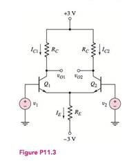
Consider the differential amplifier shown in Figure P 11.3 with transistor parameters
Want to see the full answer?
Check out a sample textbook solution
Chapter 11 Solutions
Microelectronics: Circuit Analysis and Design


- For the differential amplifier circuit below, all transistors are identical ( ?≠0 ) a) Draw the single-sided differential mode equivalent circuit, showing all details and labels Explain how you obtained this equivalent circuitarrow_forward(a) What are the Q-points for the transistors in the amplifier as shown if VDD =5V, VSS =5 V, RSS =2.4 kΩ, and RD =2.4 kΩ? Assume Kn =400 μA/V2 and VT N =0.7 V. (b) What are the differential-mode gain, common-mode gain, CMRR, and differential-mode and common-mode input resistances?arrow_forwardIn the push-pull stage given (in the photo attached), IS1 = 5 × 10⁻¹⁷ A and IS2 = 8 × 10⁻¹⁷ A. Calculate the value of VB so as to establish a bias current of 5 mA in Q1 and Q2 (for Vout = 0). If the peak input swing is 2 V and RL = 8Ω : Calculate the small-signal voltage gain for Vout ≈ 0 Use the gain obtained in (i) to estimate the output voltage swing. Estimate the peak collector current of Q1 assuming that Q2 still carries 5 mAarrow_forward
- (a) What are the Q-points for the transistors in the amplifier as shown if VCC = 12 V, VEE = 12 V, REE = 270 kΩ, RC = 330 kΩ, and βF = 100? (b) What are the differential-mode gain, and differential-mode input and output resistances? (c) What are the common-mode gain, CMRR, and common-mode input resistance for a single-ended output?arrow_forward(a) What are the Q-points for the transistors in the amplifier as shown if VCC = 15 V, VEE = 15 V, IEE = 400 μA, βF = 100, REE = 270 kΩ,RC =47 kΩ, VA=∞, and βF =100? (b) What are the differential-mode gain, common-mode gain, CMRR, and differential-mode and common-modeinput and output resistances? (c) Repeat part (b) for VA = 50 V.arrow_forwardWhat are the values of Add, Acd, and CMRR for the amplifier shown if ISS = 600 μA, RSS = 10 MΩ, Kn = Kp = 500 μA/V2, VTN =− VTP = 1 V, and λ = 0.015/V for both transistors? What are the minimum power supply voltages if the common-mode input range must be ±5 V? Assume symmetrical supply voltages.arrow_forward
- Consider the amplifier in the figure given below, where VA = 50 V, VCC = 20 V, VEE = 20 V, IEE = 350 μA, βF = 120, REE = 320 kΩ, and RC = 72 kΩ. What are the differential-mode input and output resistances of the given amplifier?arrow_forward(a) Suppose υbe(t) = 0.005 sin 2000πt V in the bipolar amplifier as shown . Write expressions for υbe(t), vce(t), and υCE(t). (b) What is the maximum value of IC that corresponds to the active region of operation?arrow_forwardInstruction/s: Draw, Illustrate and label your schematic diagram before solving the problem.2.) Given a Collector -Feedback Biased transistor circuit with voltage at common collector is +10v ,base resistor is 100k ohms, Collector resistor is 10k ohms and Base current is 8.38 micro ampere, ,Voltage at Base-emitter junction is 0.7v. Determine Beta DC , Collector current and Voltage at collector-emitter junction. These might help as a guide to answer the problem...arrow_forward
- The given circuit is a 2N4403 PNP common collector amplifier. Let VCC=12V, VEE=-12V, R1=52.5kΩ, R2=33kΩ, and RE=2.5kΩ. Determine IB, IC, IE, VB, VC, and VE. Start by initially assuming |VBE| =0.7V or and assuming a value of beta (β). Where to look for the value of β? (Hint: It’s in the transistor model assigned). Determine the input voltage (may extend from the supply voltage range) where the BJT goes from “cut-off to active” and where it goes from “active to saturation”. Assume VCE=0.3V (edge of saturation), RL=500Ω, and C1, C2→∞.arrow_forwardRefer to the differential amplifier circuit shown below . Determine the quiescent DC voltage at the collector terminal of each transistor assuming VBE of two transistor are negligible. What will be the quiescent DC values if VBE is taken to be 0.7 V.arrow_forwardThe transistor parameters for the NMOS common source amplifier given in the figure are VTN = 1.0V, kn = 0.8mA / V2 and alpha = 0. Circuit parameters are VDD = 10V, RS = 0.8k, RD = 3K, R1 = 210K and R2 = 140k. Find the IDQ drain current and VDSQ drain-source voltage at the transistor's Q - operating point. Determine in which region the transistor is operating.arrow_forward
 Introductory Circuit Analysis (13th Edition)Electrical EngineeringISBN:9780133923605Author:Robert L. BoylestadPublisher:PEARSON
 Delmar's Standard Textbook Of ElectricityElectrical EngineeringISBN:9781337900348Author:Stephen L. HermanPublisher:Cengage Learning
 Programmable Logic ControllersElectrical EngineeringISBN:9780073373843Author:Frank D. PetruzellaPublisher:McGraw-Hill Education
 Fundamentals of Electric CircuitsElectrical EngineeringISBN:9780078028229Author:Charles K Alexander, Matthew SadikuPublisher:McGraw-Hill Education
 Electric Circuits. (11th Edition)Electrical EngineeringISBN:9780134746968Author:James W. Nilsson, Susan RiedelPublisher:PEARSON
 Engineering ElectromagneticsElectrical EngineeringISBN:9780078028151Author:Hayt, William H. (william Hart), Jr, BUCK, John A.Publisher:Mcgraw-hill Education,