
Concept explainers
Videos
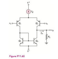
The differential amplifier shown in Figure P 11.60 has a pair of pnp bipolars as input devices and a pair of npn bipolars connected as an active load.
The circuit bias is
Want to see the full answer?
Check out a sample textbook solution
Chapter 11 Solutions
Microelectronics: Circuit Analysis and Design


- The transistor parameters for the differential amplifier shown in Figure P11.32 are VT N = 0.5 V, k n = 80 µA/V2, W/L = 4, and λ = 0. (a) Find RD and IQ such that ID1 = ID2 = 80 µA and vO2 = 2 V when v1 = v2 = 0. (b) Draw the dc load line, and plot the Q-point for M2. (c) What is the maximum common-mode input voltage? Figure p11.32arrow_forwardThe transistor parameters for the NMOS common source amplifier given in the figure are VTN = 1.0V, kn = 0.8mA / V2 and alpha = 0. Circuit parameters are VDD = 10V, RS = 0.8k, RD = 3K, R1 = 210K and R2 = 140k. Find the IDQ drain current and VDSQ drain-source voltage at the transistor's Q - operating point. Determine in which region the transistor is operating.arrow_forwardbasic amplifier circuits (base bias, voltage divider bias, emitter feedback, and collector feedback) 1. What transistor biasing provides a stable output given changes in transistor temperature?arrow_forward
- Instruction/s: Draw, Illustrate and label your schematic diagram before solving the problem.2.) Given a Collector -Feedback Biased transistor circuit with voltage at common collector is +10v ,base resistor is 100k ohms, Collector resistor is 10k ohms and Base current is 8.38 micro ampere, ,Voltage at Base-emitter junction is 0.7v. Determine Beta DC , Collector current and Voltage at collector-emitter junction. These might help as a guide to answer the problem...arrow_forwardHow a BJT works as an Amplifier? Explain in detail?arrow_forward1: Determine the value of small-signal parameter gm of Q1 for the circuit shown below.arrow_forward
- Consider the common-source amplifier shown in Figure P11.50. The NMOS transistor has KP=50 μA/V2, L=5 μm, W=500 μm, Vto=1 V and rd=∞.a. Determine the values of IDQ, VDSQ and gm. b. Compute the voltage gain, input resistance, and output resistance, assuming that the coupling capacitors are short circuits for the ac signal. Repeat Problem P11.50 for an NMOS transistor having KP=50 μA/V2, W=600 μm, L=20 μm, Vto=2 V and rd=∞. Compare the gain with that attained in Problem P11.50.arrow_forwardDesign a two-stages amplifier circuit MOSFET-BJT (no bypass for the second BJT, all BJTs are in maxswing condition)Rin=1 million Ohm, Rout=4K Ohm, Gv=15. The input signal is a sine signal, amplitude=1 V, F=1K Hz and the resistance=100K Ohmarrow_forwardThe given circuit is a 2N4403 PNP common collector amplifier. Let VCC=12V, VEE=-12V, R1=52.5kΩ, R2=33kΩ, and RE=2.5kΩ. Determine IB, IC, IE, VB, VC, and VE. Start by initially assuming |VBE| =0.7V or and assuming a value of beta (β). Where to look for the value of β? (Hint: It’s in the transistor model assigned). Determine the input voltage (may extend from the supply voltage range) where the BJT goes from “cut-off to active” and where it goes from “active to saturation”. Assume VCE=0.3V (edge of saturation), RL=500Ω, and C1, C2→∞.arrow_forward
- In the push-pull stage given (in the photo attached), IS1 = 5 × 10⁻¹⁷ A and IS2 = 8 × 10⁻¹⁷ A. Calculate the value of VB so as to establish a bias current of 5 mA in Q1 and Q2 (for Vout = 0). If the peak input swing is 2 V and RL = 8Ω : Calculate the small-signal voltage gain for Vout ≈ 0 Use the gain obtained in (i) to estimate the output voltage swing. Estimate the peak collector current of Q1 assuming that Q2 still carries 5 mAarrow_forwardIn the circuit given in the figure, Vcc = 15V, R1 = R2 = 10k ohm, RE = 1k ohm, RL = 0.5k ohm and transistor parameters are given as VBE = 0.7V, beta (dc) = beta (0) = 100. According to this;a) Calculate the values of DC bias currents and voltages (I (BQ), I (CQ), V (CEQ)).b) Using the hybrid model of the transistor, draw the small signal equivalent circuit of the circuit.c) Derive the input impedance expression of the circuit and calculate its value.d) Derive the voltage gain expressions A (vi) and A (VG) and calculate its value.e) Derive the current gain expression A (i) = I (0) / I (i) and calculate its value. I sent you question's image. Thank you..arrow_forwardNOTE: FOR ALL CIRCUITS SHOWN IN THIS QUIZ ASSUME THAT: β= 100 (for all transistors) ; Early voltage equal to infinity. 3. - For the circuit shown in figure C, determine the value of the gainAv = vo/vs Note: It is known that Vcc = 20varrow_forward
 Introductory Circuit Analysis (13th Edition)Electrical EngineeringISBN:9780133923605Author:Robert L. BoylestadPublisher:PEARSON
 Delmar's Standard Textbook Of ElectricityElectrical EngineeringISBN:9781337900348Author:Stephen L. HermanPublisher:Cengage Learning
 Programmable Logic ControllersElectrical EngineeringISBN:9780073373843Author:Frank D. PetruzellaPublisher:McGraw-Hill Education
 Fundamentals of Electric CircuitsElectrical EngineeringISBN:9780078028229Author:Charles K Alexander, Matthew SadikuPublisher:McGraw-Hill Education
 Electric Circuits. (11th Edition)Electrical EngineeringISBN:9780134746968Author:James W. Nilsson, Susan RiedelPublisher:PEARSON
 Engineering ElectromagneticsElectrical EngineeringISBN:9780078028151Author:Hayt, William H. (william Hart), Jr, BUCK, John A.Publisher:Mcgraw-hill Education,