
Videos
a.
The value of
a.
Answer to Problem 11.46P
Explanation of Solution
Given:
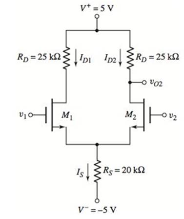
The given circuit is,
Calculation:
Consider the given figure,
Let calculate gate-to source voltage,
Now calculate source current,
Now find output voltage,
Hence,
b.
The differential-mode voltage gain and common-mode voltage gain along with CMRRdB
b.
Answer to Problem 11.46P
Explanation of Solution
Given:
The given circuit is,
Calculation:
Consider the small − signal equivalent circuit.
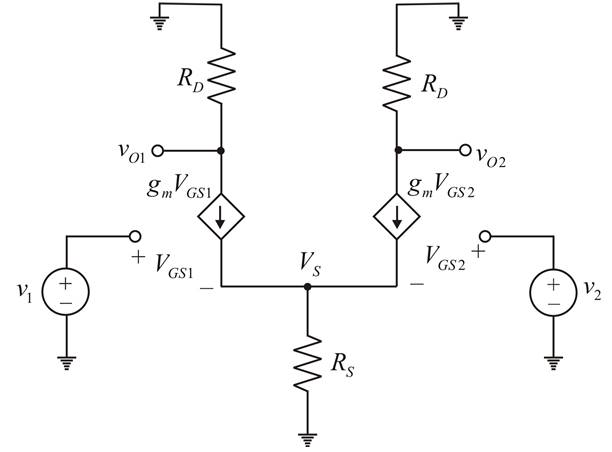
Apply KCL at node
Now,
Hence,
Want to see more full solutions like this?
Chapter 11 Solutions
Microelectronics: Circuit Analysis and Design


- 4--In the given circuit, n MOSFETs are used.Q1, Q2,….. Parameters of Qn MOS transistors Vt=1V, γ=0, λ=0,μnCox=200μA/V2 and (W/L)1=(W/L)2=….=(W/L)n=20a) VGS=?, ID=?, gm=?b) Find the input and output impedance.c) Find the voltage gain.arrow_forwardFor the circuit shown, let VCC = 3.3 V, RE = 500 Ω, RC = 4 kΩ, R1 = 85 kΩ, R2 = 35 kΩ, and β = 150. Using approximation, determine the Q-point parameters: IBQ, ICQ, and VCEQ. Indicate the exact numerical values, following the given unit.arrow_forwardDuring the turn-on and turn-off of a power transistor,the current-time and voltage-time relationshipsare as shown in the adjacent figure. Observe thewaveforms and calculate,1. The OFF-state power dissipation (static);2. The switch ON-state power dissipation(static);3. The average switching loss for the OFFtransition (dynamic);4. The average switching loss for the ONtransition (dynamic);Assume a switching frequency of 1kHz with Vx = 422Varrow_forward
- Answer as quickly as possible. I'll give upvote. Thank you. The circuit shown is a common source amplifier with a current mirror bias. It is given that the NMOS (M1) parameters are μoCox = 3mA/V2, VTH,n = 0.5V and λ = 0.02 and the PMOS (M2 and M3) parameters are μoCox = 1mA/V2 and VTH,p = −0.6V . The PMOS transistor M3 does not have channel length modulation while PMOS transistor M2 has λ = 0.02. It is also given that the dimensions of M2 and M3 have equal widths of 5µm and lengths of L2 = 3µm and L3 = 1.5µm, respectively. M1 has length of L1 = 1µm and width of W1 = 2µm. Find the gm and ro of transistor M1.arrow_forwardFor the transistors in this question, use |Vt| = 0.1V, |VA| = 10V, kn,p = 12.5mA/V2. The signal source has 0.1 mV amplitude and 1 kHz frequency. Calculate Rout, Gm and Av for the circuits separately ?arrow_forwardDetermine the folowing A.base current (IB), B. collector current (Ic), C. collector-to-emitter voltage (VCE),D. draw the load line, locate the Q-pointF. input impedance (Zi),G. Output impedance (Zo)arrow_forward
- Answer ASAP. I'll upvote. Thank you. Given: The circuit shown is a common source amplifier with a current mirror bias. It is given that the NMOS (M1) parameters are μoCox = 3mA/V2, VTH,n = 0.5V and λ = 0.02 and the PMOS (M2 and M3) parameters are μoCox = 1mA/V2 and VTH,p = −0.6V . The PMOS transistor M3 does not have channel length modulation while PMOS transistor M2 has λ = 0.02. It is also given that the dimensions of M2 and M3 have equal widths of 5µm and lengths of L2 = 3µm and L3 = 1.5µm, respectively. M1 has length of L1 = 1µm and width of W1 = 2µm. Sketch the small signal model of transistor M3 (Hint: Is there any small signal in any terminal ofM3? If yes, then where is it? If no, then what happens to the small signal model?).arrow_forwardWhat is the voltage gain of the common-emitter amplifier as shown? Assume βF = 135, VCC = VEE = 10 V, R1 = 20 kΩ, R2 = 62 kΩ,RC = 13 kΩ, and RE = 3.9 kΩ.arrow_forwardanswer all A - Explain the relation of MOSFET input current and input impedance and their effect on the functionality of the device. B- Explain how to increase the efficiency of the solar cells (PV cells) through the integration of antennas. C- List three conditions need to be considered to choose a MOSFET for switching applications.arrow_forward
- (a) For the MOSFET figure, let VDD = 15V, R1 = 4.7 MΩ, R2 = 2.2 MΩ, RS = 1kΩ, RD = 4.2kΩ, Vt = 2V, and k = 0.5 mA/V2. Find VGS, ID, and VDS. (NOTE: use Wolfram Alpha Equation Solver.) (b) Repeat with same parameters, except RS = 0.arrow_forwarda. In AC, how are the capacitors treated? b. In AC, how are DC sources treated? c. What is the amplifier configuration of Figure 4? d. What is the expected phase shift of the sinusoidal input at the output side? e. What is Zi across RG, the gate resistor? f. It is the IC in its smallest form. g. The most commonly used metal as interconnect of the chip to external peipheral. h. How is pin 1 of the chip determined? i. An IC package similar to a DIP but with the pins bent outward. j. Which sensors are packed as IC?arrow_forwardFind: 1)R1,R2 Value 2) The voltage-gain Av = Vo/Vsi , The slope of A.C.L.L 3)The value of fH due to ( CM1 & CM2) 4)If a capacitor Cs is connected across Rs then Av= 5)The value of RD required to set Q-pt at center of saturation Regn. RD= 6)The max. undistorted peak value for vds = Electronics 2arrow_forward
 Introductory Circuit Analysis (13th Edition)Electrical EngineeringISBN:9780133923605Author:Robert L. BoylestadPublisher:PEARSON
 Delmar's Standard Textbook Of ElectricityElectrical EngineeringISBN:9781337900348Author:Stephen L. HermanPublisher:Cengage Learning
 Programmable Logic ControllersElectrical EngineeringISBN:9780073373843Author:Frank D. PetruzellaPublisher:McGraw-Hill Education
 Fundamentals of Electric CircuitsElectrical EngineeringISBN:9780078028229Author:Charles K Alexander, Matthew SadikuPublisher:McGraw-Hill Education
 Electric Circuits. (11th Edition)Electrical EngineeringISBN:9780134746968Author:James W. Nilsson, Susan RiedelPublisher:PEARSON
 Engineering ElectromagneticsElectrical EngineeringISBN:9780078028151Author:Hayt, William H. (william Hart), Jr, BUCK, John A.Publisher:Mcgraw-hill Education,