
Videos
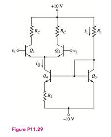
The transistor parameters for the circuit shown in Figure P 11.29 are
Want to see the full answer?
Check out a sample textbook solution
Chapter 11 Solutions
Microelectronics: Circuit Analysis and Design


- The ac equivalent circuit for an amplifier is shown. Assume the capacitors have infinite value, RI =750Ω, RB =100 kΩ, RC =100 kΩ, and R3 =100 kΩ. Calculate the input resistance and output resistance for the amplifier if the BJT Q-point is (75 μA, 10 V). Assume βo =100 and VA =75 V.arrow_forwardthe transistor in the circuit above has gm=0.11mS and ro=33Kohm. Given the following condition: R1=770Kohm, R2=890Kohm, RD=5.4Kohm, R3=20Kohm, R6=6.9Kohm, Rsig=2Kohm, determine the input impedance of the amplifier in Kohm.arrow_forwardConsider the circuit shown in Figure 11.10 on page 567. The transistor characteristics are shown in Figure 11.11. Suppose that VGG is changed to 0 V. Determine the values of VDSQ, VDSmin and VDSmax. Find the gain of the amplifier.arrow_forward
- Topic: Input and Output Characteristics of Transistor in Common Base Configuration Answer in 2-3 sentences each. Need a kind tutor that will do it for me. Thank you! 1. What are the applications of the common base (CB) configuration? 2. What are the output and input impedances of CB configuration?arrow_forward(a) What are the Q-points of the transistors in the amplifier as shown if VCC = 22 V, VEE = 22 V, I1 = 200 μA, RE = 2.4 kΩ, R = 50 kΩ, βo = 80, and VA = 70 V? (b) What are the differential-mode voltage gain and input resistance? (c) What is the amplifier output resistance? (d) What is the common-mode input resistance? (e) Which terminal is the noninverting input? (f) What is thecommon-mode input range for the amplifier if current source I1 is replaced with an electronic current source that must have 0.75 V across it to operateproperly?arrow_forwardTrue or False Increasing RE improves the CMRR for single-ended output by increasing the differential-mode gain anddecreasing the common-mode gain. Increasing RE reduces the transistor DC currents and increases the DC output voltages. The double-ended output of the differential amplifier is always zero if vs1=vs2 for any value of RE.arrow_forward
- In the push-pull stage given (in the photo attached), IS1 = 5 × 10⁻¹⁷ A and IS2 = 8 × 10⁻¹⁷ A. Calculate the value of VB so as to establish a bias current of 5 mA in Q1 and Q2 (for Vout = 0). If the peak input swing is 2 V and RL = 8Ω : Calculate the small-signal voltage gain for Vout ≈ 0 Use the gain obtained in (i) to estimate the output voltage swing. Estimate the peak collector current of Q1 assuming that Q2 still carries 5 mAarrow_forwardKnowing the equation of collector current IC for the transistor amplifier circuit, please calculate the current and voltage stabilization factors. Rc=2000ohm Re=500ohm Rb=500ohm Rb=1000ohm Beta0=200arrow_forward(a) What are the Q-points for the transistors in the amplifier as shown if VDD = 12V, VSS = 12V, ISS = 1.5 mA, RSS = 33 kΩ, and RD = 15 kΩ? Assume Kn = 375 μA/V2 and VT N = 0.75 V. (b) What are the differential-mode gain, commonmode gain, CMRR, and differential-mode and common-mode input resistances?arrow_forward
- Q.4/ Refer to the class AB power amplifier shown below:a. Determine the dc parameters VB(Q1), VB(Q2), ICQ, VCEQ(Q1), VCEQ(Q2).b. For the 5Vrms input, determine the power delivered to the load resistor.c. Determine the approximate input resistance seen by the signal source if ac=100arrow_forward1. What is the collector current of Q2 and Q1? 2. Determine the overall output resistance of the 2-stage amplifier. Do not disregard RL. 3. Determine the overall voltage gain of the 2-stage amplifierarrow_forwardProblem 1: Consider the circuit shown below. The transistor parameters are Kn1 = 0.5 mA/V2 , Kn2 = 0.2 mA/V2 , VT N1 = VT N2 = 1.2 V, and λ1 = λ2 = 0. The quiescent drain currents are ID1 = 0.2 mA and ID2 = 0.5 mA. (a) Determine the small-signal voltage gain of the given multistage amplifier. Answer: -6.14. (b) Calculate the small-signal output resistance Ro. Answer: 1.32 kΩ. Problem 2: The transistor parameters for the given circuit are β1 = 120, β2 = 80, VBE1 (on) = VBE2 (on) = 0.7 V, and VA1 = VA2 = ∞. (a) Determine the quiescent collector current in each transistor. Answer: IC1 = 2.253 mA, IC2 = 69.73 mA. (b) Find the small-signal voltage gain Av = vo/vs. Answer: 0.99. (c) Determine the input and output resistances Rib and Ro. Answer: Rib = 467.6 kΩ, Ro = 0.512 Ωarrow_forward
 Introductory Circuit Analysis (13th Edition)Electrical EngineeringISBN:9780133923605Author:Robert L. BoylestadPublisher:PEARSON
 Delmar's Standard Textbook Of ElectricityElectrical EngineeringISBN:9781337900348Author:Stephen L. HermanPublisher:Cengage Learning
 Programmable Logic ControllersElectrical EngineeringISBN:9780073373843Author:Frank D. PetruzellaPublisher:McGraw-Hill Education
 Fundamentals of Electric CircuitsElectrical EngineeringISBN:9780078028229Author:Charles K Alexander, Matthew SadikuPublisher:McGraw-Hill Education
 Electric Circuits. (11th Edition)Electrical EngineeringISBN:9780134746968Author:James W. Nilsson, Susan RiedelPublisher:PEARSON
 Engineering ElectromagneticsElectrical EngineeringISBN:9780078028151Author:Hayt, William H. (william Hart), Jr, BUCK, John A.Publisher:Mcgraw-hill Education,