
Videos
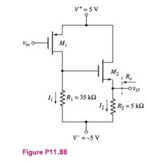
Consider the circuit in Figure
Want to see the full answer?
Check out a sample textbook solution
Chapter 11 Solutions
Microelectronics: Circuit Analysis and Design


- In order to express the effect of the internal capacitors of BJT and the high frequency reception, the current gain expression depending on the frequency (Figure b) (hfe) is used in the case of collector emitter short circuit, voltage source connected at base end and emitter grounded (Figure la).. The catalog information of the 2N2222 transistor is given in Figure Ic. In the catalogue, when Ic=20 mA, it is seen as fT=250 MHz. a) Find the total capacitor effect for the case where gm> > wCμ. (Cpi) + (Cμ) = ?pFarrow_forwardFor the transistors in this question, use |Vt| = 0.1V, |VA| = 10V, kn,p = 12.5mA/V2. The signal source has 0.1 mV amplitude and 1 kHz frequency. Calculate Rout, Gm and Av for the circuits separately ?arrow_forward1) Find the operating point of the transistor by drawing the load line of the BJT transistor circuit given below. Calculate the voltage values VE and VC. (β = 100, VBE = 0.7 V, R1 = 10 KΩ, RC = 4.7 KΩ, RE = 3.3 KΩ, VCC = 10 V, VEE = - 4 V)arrow_forward
- 2. A load of 8Ω is supplied by a single-switch Direct Current (DC) chopper with an inputvoltage of 40V. The switching frequency is 800Hz, the duty ratio is 0.4, and thetransmission voltage drop of the transistor is 2.4V a. Draw the chopper circuit presented in the question b. Find the switching period with the duty time of BJT c. Draw the load voltage, load current, BJT current, BJT voltage along two periods d. Find the output voltage. Is the achieved load voltage the average value or the effectivevalue e. Find the output power f. Find the average value and effective value of BJT current g. Find the power loss of BJT h. Find the DC source current i. Find the circuit efficiencyarrow_forwardVs=100 mV peak-to-peak, 1 kHz sine signal, Kn=0.4mA/v^2 ,Vt=1V , λ=0.01V^-1 Make the DC analysis of the above given mosfet amplifier circuit. Simulation to tableWrite down the measured values and mathematical calculation results. (The valueswith the units.)DC Parameters ,Measured value ,Calculated ValueVGETCVGSVDVDSIDb. Draw the small signal model for the AC analysis of the circuit. Find the gm, ro, Av values.c. Show the Vs input signal and the Vo output signal of the circuit on the oscilloscope. Volt/div of channels andSpecify time/div values.arrow_forwardA MOSFET common-source amplifier must amplify a sinusoidal ac signal with a peak amplitude of 0.4 V. What is the minimum value of VGS −VT Nfor the transistor? If a voltage gain of 26 dB is required, what is the minimum power supply voltage?arrow_forward
- The ac equivalent circuit for an amplifier is shown. Assume the capacitors have infinite value, RI =750Ω, RB =100 kΩ, RC =100 kΩ, and R3 =100 kΩ. Calculate the input resistance and output resistance for the amplifier if the BJT Q-point is (75 μA, 10 V). Assume βo =100 and VA =75 V.arrow_forwardIf RB=12KΩ, RC=150Ω, VBB=7V, VCC=18V determine the IB, IC, IE and collector – emitter voltage in the circuit given below. The transistor has a gain (β) =150. Assume forward voltage drop of the BE junction is 0.7 V (Fig Q2 (d))arrow_forwardThe dc bias circuit for a common emitter amplifier is shown in the figure. In the circuit, Vcc=15v,RB1=20k Ω,RB2=100k Ω,Rc=5.1k Ω,and RE1=1k Ω, Assume that when the transistor is on, the voltage drop from base to emitter VBE=0.7v. Also assume that β= ∞, which implies that the base current can be considered zero (IB=0) in your calculations. Solve for the base voltage VB. Solve for the emitter voltage VE. Solve for the emitter current IB. Solve for the collector current ICarrow_forward
- For the BJT amplifier circuit of figure below with the following parameters:β = hfe ≈ 250, re= 20.3Ω, and ro = 1/hoe ≈ ∞ Ω, Zb= 50.26KΩ determine:(a) Draw the Ac equivalent circuit in re- model and hybrid model.(b) hie, , Zi , and Zo'(c) Av using h- model.(d) Avs and ac output voltagearrow_forwardGiven the BJT bias circuit given below, solve for I_E, I_B, I_C, V_O, and β using the circuit parameters given in Table 1. Determine and verify the operating region of the BJT transistor. Draw the small-signal model of the circuit and solve for the small signal parameters rπ, gm, and ro. Let R_C = 12kΩ, R_B = 30kΩ, R_E = 2.5kΩ, and V_A = 50V. V_EB = 0.8V V_CC = 0V V_EE = -25V I_RC = 1.65mAarrow_forwardKnowing the equation of collector current IC for the transistor amplifier circuit, please calculate the current and voltage stabilization factors. Rc=2000ohm Re=500ohm Rb=500ohm Rb=1000ohm Beta0=200arrow_forward
 Introductory Circuit Analysis (13th Edition)Electrical EngineeringISBN:9780133923605Author:Robert L. BoylestadPublisher:PEARSON
 Delmar's Standard Textbook Of ElectricityElectrical EngineeringISBN:9781337900348Author:Stephen L. HermanPublisher:Cengage Learning
 Programmable Logic ControllersElectrical EngineeringISBN:9780073373843Author:Frank D. PetruzellaPublisher:McGraw-Hill Education
 Fundamentals of Electric CircuitsElectrical EngineeringISBN:9780078028229Author:Charles K Alexander, Matthew SadikuPublisher:McGraw-Hill Education
 Electric Circuits. (11th Edition)Electrical EngineeringISBN:9780134746968Author:James W. Nilsson, Susan RiedelPublisher:PEARSON
 Engineering ElectromagneticsElectrical EngineeringISBN:9780078028151Author:Hayt, William H. (william Hart), Jr, BUCK, John A.Publisher:Mcgraw-hill Education,