
Videos
Consider the diff-amp with active load in Figure P11.66. The Early voltages are
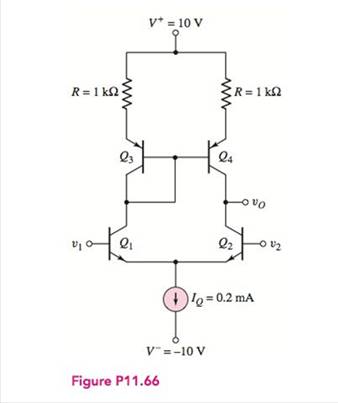
(a) Determine the open-circuit differential-mode voltage gain. (b) Compare this value to the gain obtained when
Want to see the full answer?
Check out a sample textbook solution
Chapter 11 Solutions
Microelectronics: Circuit Analysis and Design


- The transistor parameters for the NMOS common source amplifier given in the figure are VTN = 1.0V, kn = 0.8mA / V2 and alpha = 0. Circuit parameters are VDD = 10V, RS = 0.8k, RD = 3K, R1 = 210K and R2 = 140k. Find the IDQ drain current and VDSQ drain-source voltage at the transistor's Q - operating point. Determine in which region the transistor is operating.arrow_forwardWhat change(s), if any, can be introduced into the circuit shown below for a) zero bias? b) depletion- mode bias? c) enhancement- mode bias?arrow_forwardNOTE: FOR ALL CIRCUITS SHOWN IN THIS QUIZ ASSUME THAT: β= 100 (for all transistors) ; Early voltage equal to infinity. 3. - For the circuit shown in figure C, determine the value of the gainAv = vo/vs Note: It is known that Vcc = 20varrow_forward
- NOTE: FOR ALL CIRCUITS SHOWN IN THIS QUIZ ASSUME THAT: β= 100 (for all transistors) ; Early voltage equal to infinity. 2. - For the circuit shown in figure B, determine:a) The values of IcQ and VceQ for Q1 and Q2b) The input resistance Ri and the output resistance Roarrow_forwardConsider the common-source amplifier shown in Figure P11.50. The NMOS transistor has KP=50 μA/V2, L=5 μm, W=500 μm, Vto=1 V and rd=∞.a. Determine the values of IDQ, VDSQ and gm. b. Compute the voltage gain, input resistance, and output resistance, assuming that the coupling capacitors are short circuits for the ac signal. Repeat Problem P11.50 for an NMOS transistor having KP=50 μA/V2, W=600 μm, L=20 μm, Vto=2 V and rd=∞. Compare the gain with that attained in Problem P11.50.arrow_forwardQ.1/ Figure below shows a CE power amplifier in which the collector resistor serves also as the load resistor. Assume DC=ac=100.a. Determines the dc Q-point (ICQ and VCEQ).b. Determine the voltage gain and the power gain.c. What changes would be necessary to convert the circuit to a pnp transistor with a positive supply? What advantage would this have?arrow_forward
- Given that the enhancement transistor shown in Figure P11.14 has Vto=1 V and K=0.5 mA/V2. find the value of the resistance R.arrow_forwardDescribe the purpose and operating principle of UJT (unijunction transitor) and SCR amplifiersarrow_forwardEach of the transistors shown in Figure P12.34 has β=100, |VCE|=0.2 V in saturation, and |VBE|=0.6 V in the active and saturation regions. For each transistor, determine the region of operation and the values of VCE, IB, IE and IC.arrow_forward
- In the circuit given in the figure, Vcc = 15V, R1 = R2 = 10k ohm, RE = 1k ohm, RL = 0.5k ohm and transistor parameters are given as VBE = 0.7V, beta (dc) = beta (0) = 100. According to this;a) Calculate the values of DC bias currents and voltages (I (BQ), I (CQ), V (CEQ)).b) Using the hybrid model of the transistor, draw the small signal equivalent circuit of the circuit.c) Derive the input impedance expression of the circuit and calculate its value.d) Derive the voltage gain expressions A (vi) and A (VG) and calculate its value.e) Derive the current gain expression A (i) = I (0) / I (i) and calculate its value. I sent you question's image. Thank you..arrow_forwardShown in Figure P12.17 is the Darlington pair, which is equivalent to a single transistor, as indicated in the figure. Assuming that both Q1 and Q2 are operating in the active region, with |VBE|= 0.6 V, determine the value for VBE for the equivalent transistor in the active region. Repeat for the Sziklai pair shown in Figure P12.28.arrow_forwardInstruction/s: Draw, Illustrate and label your schematic diagram before solving the problem.2.) Given a Collector -Feedback Biased transistor circuit with voltage at common collector is +10v ,base resistor is 100k ohms, Collector resistor is 10k ohms and Base current is 8.38 micro ampere, ,Voltage at Base-emitter junction is 0.7v. Determine Beta DC , Collector current and Voltage at collector-emitter junction. These might help as a guide to answer the problem...arrow_forward
 Introductory Circuit Analysis (13th Edition)Electrical EngineeringISBN:9780133923605Author:Robert L. BoylestadPublisher:PEARSON
 Delmar's Standard Textbook Of ElectricityElectrical EngineeringISBN:9781337900348Author:Stephen L. HermanPublisher:Cengage Learning
 Programmable Logic ControllersElectrical EngineeringISBN:9780073373843Author:Frank D. PetruzellaPublisher:McGraw-Hill Education
 Fundamentals of Electric CircuitsElectrical EngineeringISBN:9780078028229Author:Charles K Alexander, Matthew SadikuPublisher:McGraw-Hill Education
 Electric Circuits. (11th Edition)Electrical EngineeringISBN:9780134746968Author:James W. Nilsson, Susan RiedelPublisher:PEARSON
 Engineering ElectromagneticsElectrical EngineeringISBN:9780078028151Author:Hayt, William H. (william Hart), Jr, BUCK, John A.Publisher:Mcgraw-hill Education,