
(a)
The value of the output resistance.
(a)
Answer to Problem 11.70P
The value of the output resistance
Explanation of Solution
Given:
The given diagram is shown in Figure 1

Figure 1
Calculation:
The expression for the input current is given by,
The expression to determine the value of the transconductance is given by,
The expression for the relation for the voltage for hybrid pie parameter.
Substitute
The value of the collector current
The value of the collector current
The expression to determine the expression for the diffusion resistance is given by,
Substitute
The value of the transconductance is calculated as,
Substitute
The expression to determine the value of the resistance
Substitute
The expression to determine the expression for the diffusion resistance is given by,
Substitute
The value of the transconductance is calculated as,
Substitute
The expression to determine the value of the resistance
Substitute
Substitute
The expression for the input current
Substitute
Substitute
The expression to determine the output resistance is given by,
Substitute
The value of the quiescent current is given by,
The small signal output resistance is calculated as,
The value of the output resistance is calculated as,
Conclusion:
Therefore, the value of the output resistance
(b)
The value of the differential mode voltage gain.
(b)
Answer to Problem 11.70P
The value of the differential voltage gain is
Explanation of Solution
Given:
The given diagram is shown in Figure 1
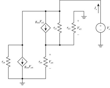
Figure 1
Calculation:
The required small signal circuit is shown in Figure 2
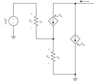
Figure 2
The expression for the transconductance is given by,
The expression for the differential voltage gain is given by,
The expression for the change in current is given by,
Consider the value of
Substitute the values in the above equation.
Substitute
Substitute
Substitute
Substitute
The value of gain is given by,
The expression for the input resistor is given by,
The value of expression for the differential input resistor is calculated as,
Conclusion:
Therefore, the value of the differential voltage gain is
(c)
The value of the differential mode input resistance
(c)
Answer to Problem 11.70P
The value of
Explanation of Solution
Given:
The given diagram is shown below.

Calculation:
The expression for the input resistor is given by,
The value of expression for the differential input resistor is calculated as,
Conclusion:
Therefore, the value of
Want to see more full solutions like this?
Chapter 11 Solutions
Microelectronics: Circuit Analysis and Design

- For the class B output stage of Figure 2, let ??? = 6 V and ?? = 4Ω. If the output is a sinusoidal with 4.5V peak amplitude, find; (a) The output power. (b) The average power drawn from each supply/ (c) The power efficiency obtained at this output voltage. (d) The maximum power that each transistor must be capable of dissipating safely.arrow_forwardEach of the transistors shown in Figure P12.34 has β=100, |VCE|=0.2 V in saturation, and |VBE|=0.6 V in the active and saturation regions. For each transistor, determine the region of operation and the values of VCE, IB, IE and IC.arrow_forwardNOTE: FOR ALL CIRCUITS SHOWN IN THIS QUIZ ASSUME THAT: β= 100 (for all transistors) ; Early voltage equal to infinity. 3. - For the circuit shown in figure C, determine the value of the gainAv = vo/vs Note: It is known that Vcc = 20varrow_forward
- NOTE: FOR ALL CIRCUITS SHOWN IN THIS QUIZ ASSUME THAT: β= 100 (for all transistors) ; Early voltage equal to infinity. 2. - For the circuit shown in figure B, determine:a) The values of IcQ and VceQ for Q1 and Q2b) The input resistance Ri and the output resistance Roarrow_forwardWhat type of biasing circuit using in the common source JFET amplifier?arrow_forwardGiven the circuit of Figure P10.6, determine theoperating point of the transistor. Assume a 0.6-V offsetvoltage and β = 150. In what region is the transistor?arrow_forward
- The transistors shown in Figure P12.43 operate in the active region and have β=100 and VBE=0.7 V. Determine IC and VCE for each transistor.arrow_forwardDescribe the working principles of Bipolar Junction Transistor (BJT): Study of Single Stage Transistor Common Emitter Amplifierarrow_forwardDescribe the purpose and operating principle of UJT (unijunction transitor) and SCR amplifiersarrow_forward
- How a BJT works as an Amplifier? Explain in detail?arrow_forwardThe transistor having the characteristics shown in Figure P12.18 is operating with iC=8 mA and vCE = 12 V. Locate the point of operation on both the input and output characteristics.arrow_forwardTopic: Field Effect Transistor Given the FET Amplifier circuit. Answer the question asked in each letter. a. Transconductance Gain (gm) b. Drain Resistor (RD) c. Input Impedance (Zi) d. Output Impedance (Zo) e. Voltage Gain (Av) f. What is the AC configuration of the amplifier?common source, common gate, common drain, or source bias?arrow_forward
 Introductory Circuit Analysis (13th Edition)Electrical EngineeringISBN:9780133923605Author:Robert L. BoylestadPublisher:PEARSON
 Delmar's Standard Textbook Of ElectricityElectrical EngineeringISBN:9781337900348Author:Stephen L. HermanPublisher:Cengage Learning
 Programmable Logic ControllersElectrical EngineeringISBN:9780073373843Author:Frank D. PetruzellaPublisher:McGraw-Hill Education
 Fundamentals of Electric CircuitsElectrical EngineeringISBN:9780078028229Author:Charles K Alexander, Matthew SadikuPublisher:McGraw-Hill Education
 Electric Circuits. (11th Edition)Electrical EngineeringISBN:9780134746968Author:James W. Nilsson, Susan RiedelPublisher:PEARSON
 Engineering ElectromagneticsElectrical EngineeringISBN:9780078028151Author:Hayt, William H. (william Hart), Jr, BUCK, John A.Publisher:Mcgraw-hill Education,