
Concept explainers
Videos
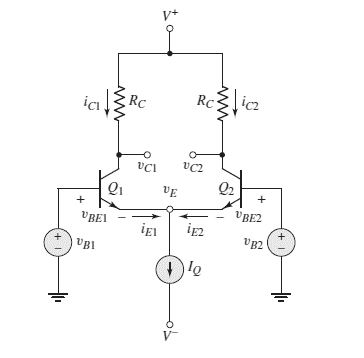
The circuit parameters for the differential amplifier shown in Figure 11.2 are
a.
The collector voltages, collector to emitter voltages and the emitter voltage for the given input values of a differential amplifier.
Answer to Problem 11.1EP
Explanation of Solution
Given Information:
The given values are:
The given circuit is shown below.
Calculation:
Voltage at emitter of each transistor
Assume transistors are matched. Then,
Also assume that the bias currents are negligible. Then,
Now
Then,
Similarly,
b.
The collector voltages, collector to emitter voltages and the emitter voltage for the given values of a differential amplifier.
Answer to Problem 11.1EP
Explanation of Solution
Given Information:
The given values are:
The given circuit is shown below.

Calculation:
Voltage at emitter of each transistor
Assume transistors are matched. Then,
Also assume the bias currents are negligible. Then,
Now
Then,
Similarly,
c.
The collector voltages, collector to emitter voltages and the emitter voltage for the given values of differential amplifier.
Answer to Problem 11.1EP
Explanation of Solution
Given Information:
The given values are:
The given circuit is shown below.

Calculation:
Voltage at emitter of each transistor
Assume transistors are matched. Then,
Also assume the bias currents are negligible. Then,
Now
Then,
Similarly,
Want to see more full solutions like this?
Chapter 11 Solutions
Microelectronics: Circuit Analysis and Design


- The ac equivalent circuit for an amplifier is shown. Assume the capacitors have infinite value, RI = 100 kΩ, RG = 10 MΩ, RD = 560 kΩ, and R3 = 1.5 MΩ. Calculate the voltage gain for the amplifier if the MOSFETQ-point is (10 μA, 5 V). Assume Kn = 100 μA/V2 and λ = 0.02 V−1.arrow_forwardthe transistor in the circuit above has gm=0.11mS and ro=33Kohm. Given the following condition: R1=770Kohm, R2=890Kohm, RD=5.4Kohm, R3=20Kohm, R6=6.9Kohm, Rsig=2Kohm, determine the input impedance of the amplifier in Kohm.arrow_forwardThe ac equivalent circuit for an amplifier is shown. Assume the capacitors have infinite value, RI = 100 kΩ, RG = 6.8MΩ, RD = 50 kΩ, and R3 = 120 kΩ. Calculate the voltage gain for the amplifier if the MOSFET Q-point is (100 μA, 5 V). Assume Kn = 450 μA/V2 and λ = 0.02 V−1.arrow_forward
- The ac equivalent circuit for an amplifier is shown. Assume the capacitors have infinite value, RI =750Ω, RB =100 kΩ, RC =100 kΩ, and R3 =100 kΩ. Calculate the input resistance and output resistance for the amplifier if the BJT Q-point is (75 μA, 10 V). Assume βo =100 and VA =75 V.arrow_forwardConsider the common-source amplifier shown in Figure P11.50. The NMOS transistor has KP=50 μA/V2, L=5 μm, W=500 μm, Vto=1 V and rd=∞.a. Determine the values of IDQ, VDSQ and gm. b. Compute the voltage gain, input resistance, and output resistance, assuming that the coupling capacitors are short circuits for the ac signal. Repeat Problem P11.50 for an NMOS transistor having KP=50 μA/V2, W=600 μm, L=20 μm, Vto=2 V and rd=∞. Compare the gain with that attained in Problem P11.50.arrow_forwardThe ac equivalent circuit for an amplifier is shown . Assume the capacitors have infinite value, RI = 10 kΩ, RB = 5 MΩ, RC = 1.5 MΩ, and R3 = 3.3 MΩ. Calculate the input resistance and output resistance for the amplifier if the BJT Q-point is (2 μA, 2 V). Assume βo = 40 and VA = 50 V.arrow_forward
- If the circuit of problem 2 is configured as a common-emitter amplifier, calculate the resulting voltage and current gain. Assume a load resistor of 1k ohm. Circuit of problem 2: determine the operating point of a universal trasnsistor DC bias cirucit when Vcc=15V, R1=10k ohm, R2=2.2k ohm, Rc=680 ohm, Re=100 ohm. Assume beta (b)=200 and Vbe=0.72V.arrow_forwardGiven the differential amplifier circuit below. Determine the following: emitter current, differential mode voltage gain, common mode voltage gain and CMRR.arrow_forwardSince the transistors used in the circuit are B=100, ro=∞ a) Find the re1, re2 resistance values by performing the DC analysis for each amplifier stage separately. b) Draw the AC equivalent circuit of the amplifier circuit. c)Find the input and output impedance values for each amplifier stage. d) Find the voltage gains AV1, AV2 for each amplifier stage. e) Find the voltage value VL by finding the AV1 Voltage gain.arrow_forward
- True or False Increasing RE improves the CMRR for single-ended output by increasing the differential-mode gain anddecreasing the common-mode gain. Increasing RE reduces the transistor DC currents and increases the DC output voltages. The double-ended output of the differential amplifier is always zero if vs1=vs2 for any value of RE.arrow_forwardSince Vcc = 12 V, Vin = 690 mV, RB = 780 kΩ, RC1 = 27.9 Ω, RC2 = 25.4 Ω, RE = 470 Ω, RL = 47 Ω and β1 = β2 = 100 in the circuit in the figure Find the current (IL) flowing through RL? NOTE-1: VBE1 = VBE2 = 0.7 V will be taken. NOTE-2: Output impedances of transistors (r0) will be neglected.arrow_forwardA common-source amplifier with a drain resistance, RD = 4.7 k Ω, is powered using a10 V power supply. Assuming that the transconductance, gm, is 520 μA/V, the voltage gain of the amplifier is closest to:arrow_forward
 Introductory Circuit Analysis (13th Edition)Electrical EngineeringISBN:9780133923605Author:Robert L. BoylestadPublisher:PEARSON
 Delmar's Standard Textbook Of ElectricityElectrical EngineeringISBN:9781337900348Author:Stephen L. HermanPublisher:Cengage Learning
 Programmable Logic ControllersElectrical EngineeringISBN:9780073373843Author:Frank D. PetruzellaPublisher:McGraw-Hill Education
 Fundamentals of Electric CircuitsElectrical EngineeringISBN:9780078028229Author:Charles K Alexander, Matthew SadikuPublisher:McGraw-Hill Education
 Electric Circuits. (11th Edition)Electrical EngineeringISBN:9780134746968Author:James W. Nilsson, Susan RiedelPublisher:PEARSON
 Engineering ElectromagneticsElectrical EngineeringISBN:9780078028151Author:Hayt, William H. (william Hart), Jr, BUCK, John A.Publisher:Mcgraw-hill Education,