
Videos
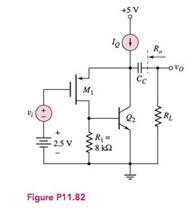
The BiCMOS circuit shown in Figure P11.82 is equivalent to a pnp bipolar transistor with an infinite input impedance. The bias current is
(a)
To sketch: The small-signal equivalent circuit of the given BiCMOS circuit.
Answer to Problem 11.82P
The required sketch is shown in Figure 3.
Explanation of Solution
Given:
The given diagram is shown below.

Calculation:
Mark the value and redraw the circuit.
The required diagram is shown in Figure 1
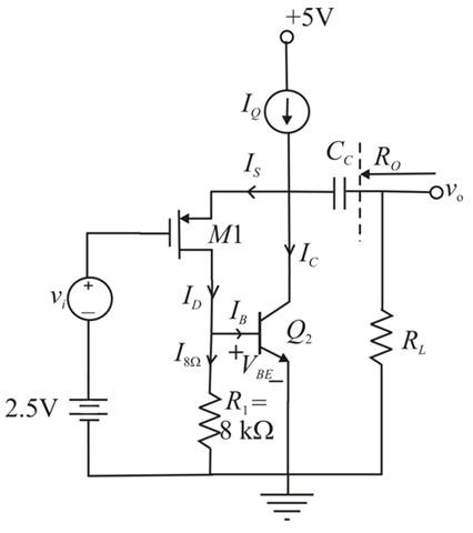
Figure 1
The small signal equivalent circuit is shown in Figure 2
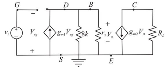
Figure 2
Conclusion:
Therefore, the required sketch is shown in Figure 2
(b)
The small signal parameters for each of the transistor.
Answer to Problem 11.82P
The value of small signal parameters are
Explanation of Solution
iven:
The given diagram is shown below.
Calculation:
The value of the current through the resistance
The expression for the resistance
Substitute
The value of the drain current is calculated as,
The expression for the collector current is given by,
Substitute
The value of the base current is calculated as,
The transconductance of the first transistor is given by,
Substitute
The transconductance of the first transistor is given by,
Substitute
The value of the resistance
Conclusion:
Therefore, the value of small signal parameters are
(c)
The value of small signal voltage gain for the given values of load resistor.
Answer to Problem 11.82P
The value of the small signal voltage gain for
Explanation of Solution
Given:
The given diagram is shown below.

The given values of load resistor is
Calculation:
The expression for the voltage
The expression for the gate to source voltage is given by,
The expression to determine the value of the output voltage is given by,
Substitute
Substitute
Conclusion:
Therefore, the value of the small signal voltage gain for
Want to see more full solutions like this?
Chapter 11 Solutions
Microelectronics: Circuit Analysis and Design


- Given the BJT bias circuit, solve for IE, IB, IC, VO, and β. Let RC=12kΩ, RB=30kΩ, RE=2.5kΩ, VA=50V, VEB=0.7V, VCC=15V, VEE=–15V, and IRC=2mA.arrow_forwardGiven an FM modulator with a deviation sensitivity K1= 3.7 kHz/V and a modulating signal vm = 5.2 sin(2π1,906t), determine the carrier swing in kHz For an FM modulator with an unmodulated carrier amplitude Vc= 14 V, a modulation index m = 1, and a load resistance RL = 8 ohms, determine the power (in watts) in the modulated carrier The percent modulation of the sound portion of a TV signal is 85%. The maximum frequency deviation for the sound portion of the TV signal as specified by the FCC is 25 kHz. Determine the carrier swing (in kHz) of the signal. For an FM modulator with 40-kHz frequency deviation and a modulating-signal frequency fm= 13 kHz, determine the bandwidth (in kHz) using Carson's rule. Given an FM modulator with a deviation sensitivity K1= 1.4 kHz/V and a modulating signal vm = 3.9 sin(2π1,948t), determine the peak frequency deviation in kHz. The percent modulation of the sound portion of a TV signal is 73%. The maximum frequency deviation for the sound portion of the…arrow_forwardFor a mosfet amplifier circuit, how can I choose an input and output capacitor with poles at 10Hz and 100Hz? Where RC = 1/w.arrow_forward
- For an FM modulator with unmodulated carrier amplitude of Vc = 20cos(2π600Mhz t) and modulating signal of Vm= 8cos(2π10KHz t) a frequency deviation of 15kHz, and a load resistance RL = 10ohms. Determine the total power of the side frequencies A. 14.808W B. 0.1851W C. 0.93W D. 7.404arrow_forward2. The SNRo of a receiver is determined to be 35.937dB. Determine the SNRi in dB, if the modulation index is kept at 2 and the modulating signal is determined to have a peak voltage of 12.452. It is also noted that the system's sensitivity to changes in frequency is 200.718Hz/V. This modulator is using the maximum frequency deviation.arrow_forwardQ23) This multiple choice question from DIGITAL COMMUNICATIONS course.just write for me the final answer. A baseband system has a signal-to-noise ratio of 100 and a bandwidth efficiency of 1.25 .The average bit energy to noise spectral density of this system is equal to------- a)80 b)160 c)125 d)250arrow_forward
- 1.Select the correct statement(s) regarding frequency modulation (FM) bandwidth. a. the more the carrier frequency is allowed to change frequencies (Δf), the smaller the modulated signal bandwidth b. the larger the FM index, β, the larger the modulated signal bandwidth c. as you increase kvco, you decrease modulated signal bandwidth d. all statements are correct 2. Select the correct statement(s) regarding baseband signal modulation. a. with modulation, a baseband signal can be moved to a higher frequency thus preventing baseband signal interference b. modulation techniques are only required for analog information signals, since digital signals are represented by discrete logical values of “1” and “0” c. modulation eliminates the baseband signal’s frequency bandwidth, thus enabling greater efficiencies when transmitting a modulated carrier signal d. all statements are correct 3. A…arrow_forwardDraw block diagram /circuit diagram of the ff. FM circuits and discuss the operation. b. FOSTER SEELEY DISCRIMINATORarrow_forward(a) The signal voltage applied across the gatesource terminals of an MOS transistor is given by υgs = VM sin 5000πt, and VGS − VT N = 0.75 V.Calculate the total harmonic distortion in the drain current of the MOSFET based upon Eq. 13.70 if VM = 150 mV. (b) repeat for VM = 300 mV.(c) Repeat for VM = 75 mV.arrow_forward
- 3. (a) The overall Noise Figure (NF) of a 2 –stage cascaded receiver is given as 35dB.The gain of the first stage is 4dB and the Noise Figure of the first stage is 28 dB.Find the noise figure and the equivalent noise temperature of the second stage.Assume the reference temperature is 17oC. (b) In a multi stage cascaded receiver, which stage mostly determines the overall NoiseFigure? Explain why. note: the answer will be by hand written.arrow_forwardFor the transistors in this question, use |Vt| = 0.1V, |VA| = 10V, kn,p = 12.5mA/V2. The signal source has 0.1 mV amplitude and 1 kHz frequency. Calculate Rout, Gm and Av for the circuits separately ?arrow_forward1. What is the order of the RC filter transfer function? 3rd 2nd 4th 1st 2. Why are unity gain amplifiers used? To separate complicated chains in signal transmission into separate simple circuits To filter the signal To amplify the signal To “condition the signal” so there is no voltage dividersarrow_forward
 Introductory Circuit Analysis (13th Edition)Electrical EngineeringISBN:9780133923605Author:Robert L. BoylestadPublisher:PEARSON
 Delmar's Standard Textbook Of ElectricityElectrical EngineeringISBN:9781337900348Author:Stephen L. HermanPublisher:Cengage Learning
 Programmable Logic ControllersElectrical EngineeringISBN:9780073373843Author:Frank D. PetruzellaPublisher:McGraw-Hill Education
 Fundamentals of Electric CircuitsElectrical EngineeringISBN:9780078028229Author:Charles K Alexander, Matthew SadikuPublisher:McGraw-Hill Education
 Electric Circuits. (11th Edition)Electrical EngineeringISBN:9780134746968Author:James W. Nilsson, Susan RiedelPublisher:PEARSON
 Engineering ElectromagneticsElectrical EngineeringISBN:9780078028151Author:Hayt, William H. (william Hart), Jr, BUCK, John A.Publisher:Mcgraw-hill Education,