
Videos
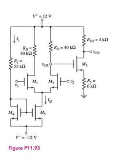
For the transistors in the circuit in Figure
(a)
The values of the differential mode voltage gain and the common mode voltage gain for the given transistor circuit.
Answer to Problem 11.93P
The differential-mode voltage gain is
The common-mode voltage gain is
Explanation of Solution
Given:
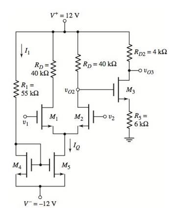
The given circuit is shown below.
The transistor parameters are:
Calculation:
The small signal model of the given transistor circuit is shown below:
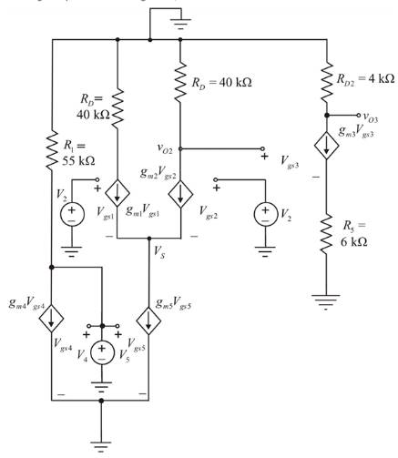
The value of the gate-source voltage of the transistor 4 is calculated as shown below:
The quiescent current is,
The value of the gate-source voltage of the transistor 3 is calculated as shown below:
The transconductance parameters for the differential gain are calculated as shown below:
The differential gain is,
The common mode gain is,
(b)
The values of the output voltage for the given input voltages.
To compare: The result with the ideal case.
Answer to Problem 11.93P
The output voltage is
Explanation of Solution
Given:
The given circuit is shown below.

The circuit parameters are:
Calculation:
The output voltage is calculated as shown below:
On comparing the above output voltage with the ideal case,
Want to see more full solutions like this?
Chapter 11 Solutions
Microelectronics: Circuit Analysis and Design


- Q/ If two signals of the same amplitude and frequency (1V, 20KHz) are simultaneously inserted into the first and second channel, the phase difference o between them 36 , while the time basis and sensitivity of the vertical amplifier were div/10µsec, div/v 5.0 on straight. Draw the expected waveforms.?arrow_forwardVcc=25V , Vi=35mV , RB =470kΩ , RC=2,6kΩ , RE1=470Ω , RE2=1.2kΩ , RL=16.8kΩ , β=110 Find the output voltage V0 = ? Note1=Capacitors are negligible at mid-band frequency. Note2 0 The output impedance (r0) of the transistor will be neglected.arrow_forwardCalculate the harmonic distortion component for an output signal having a fundamental amplitude of 3 V and a second harmonic amplitude of 0.25 V.arrow_forward
- ı just need the fınal answer Since Vcc = 20 V, RS = 3 kΩ, RB = 380 kΩ, RC = 1.2 kΩ, RE = 2.2 kΩ, RL = 911 Ω and β = 90 in the circuit in the figure, find the value of the output voltage (Vo). NOTE-1: It is within the 1 kHz mid-band frequency and the capacitors are negligible at this frequency. NOTE-2: The output impedance (r0) of the transistor will be neglected. a. 64,14 mV b. 83,88 mV c. 93,75 mV d. 74,01 mV e. 103,62 mV f. 24,67 mV g. 34,54 mV h. 49,34 mVarrow_forwardDraw the DC circuit: b)DC computations: Compute the DC collector current of each transistor. I_C 1 = ________________________ mA I_C 2= ________________________ Calculations: c)Draw the AC circuit and compute gm, r_pi for the system. g_m 1= _______________________ mA/V r_pi 1 = _______________________ kohms g_m 2= _______________________ mA/V r_pi 2 = _______________________ kohms AC circuit: Calculations: d)Compute the gain A_v=Vo/Vi at the operational band (for sufficiently high frequency) Gain = A_v = ______________________________ Computations:arrow_forwardDetermine its sensitivity value, then if S changes from 100 to 120 what is the percentage effect to the entire system's performancearrow_forward
- In the circuit shown in the figure, Vcc = 12 V, Vin = 10 mV, β = 100, r0 = 40 kΩ, RB = 360 kΩ, RC = 3.3 kΩ, RE = 220 Ω, Rs = 0.5 kΩ and RL = 7.1 kΩ . Accordingly, find the voltage gain (Vout/Vin) of the circuit. NOTE-1: The output impedance of the transistor r0 will be taken into account in the calculations.NOTE-2: Capacitors are negligible at midband frequency.arrow_forwardElectronic Since k = 0.35x10^3, VGSQ = 6.2 V, VGS(Th) = 2.4 V, RF = 100 MΩ, RG = 10 MΩ, RD = 7.6 kΩ, RS = 2.2 kΩ and RL = 21 kΩ in the circuit in the figure, the output voltage In which option is the amplitude value (Vout) given correctly? NOTE-1: E-MOSFET output impedance is rd = 70 kΩ and should be taken into account in calculations. NOTE-2: Capacitors are of negligible size at mid-band frequency. NOTE-3: It is within the 5 kHz mid-band frequency.arrow_forwardIn the circuit shown in the figure, Vcc = 12 V, Vin = 10 mV, β = 100, r0 = 40 kΩ, RB = 360 kΩ, RC = 3.3 kΩ, RE = 220 Ω, Rs = 0.5 kΩ and RL = 42.1 kΩ . Accordingly, find the voltage gain (Vout/Vin) of the circuit.NOTE-1: The output impedance of the transistor r0 will be taken into account in the calculations.NOTE-2: Capacitors are negligible at midband frequency.arrow_forward
- What is the modulation index for an AM signal having Vmax and Vmin of 2.6 and 0.29, respectively Answer: 0.799 show the solutionarrow_forward1. The high frequency response of an RC coupled amplifier depends on: a) The input coupling capacitors b) The midrange voltage gain The bypass capacitor d) The output coupling capacitors 2. IM the peak output voltage of an amplifier at the critical frequency is 20 V. the output voltage at midrange is: a) 17 V b) 23 V c) 14.14 V d) 28.3V 3. The low frequency response of RC coupled BJT amplifier depends on 1.) The bypass capacitor b) l'he input and output capacitors c) The input coupling capacitor d) All capacitors in the circuit +. The input Miller capacitance of a BJT amplifier depends partly on: a) Inpui coupling capacitor b) The voltage gain at lower critical frequency ) The internal capacitances of the transistor d) the bypass capacitor 5 When the frequency of an amplifier is reduced linearly from 100 kHz to 1 kHz. the gain of the amplilier is reduced by 12 213. then the roll-off rate is: a)-12 dB/octave b) - 12 dB/ decade c) -6 dB/ decade d) -6 dB/octave 6. A multistage amplifier…arrow_forwardWhat is the minimum bandwidth of the pnp current mirror as shown if IS = 80 μA, βo = 50, VA = 60 V, fT = 50 MHz, Cμ = 2.5 pF, and AE2 = AE1?arrow_forward
 Introductory Circuit Analysis (13th Edition)Electrical EngineeringISBN:9780133923605Author:Robert L. BoylestadPublisher:PEARSON
 Delmar's Standard Textbook Of ElectricityElectrical EngineeringISBN:9781337900348Author:Stephen L. HermanPublisher:Cengage Learning
 Programmable Logic ControllersElectrical EngineeringISBN:9780073373843Author:Frank D. PetruzellaPublisher:McGraw-Hill Education
 Fundamentals of Electric CircuitsElectrical EngineeringISBN:9780078028229Author:Charles K Alexander, Matthew SadikuPublisher:McGraw-Hill Education
 Electric Circuits. (11th Edition)Electrical EngineeringISBN:9780134746968Author:James W. Nilsson, Susan RiedelPublisher:PEARSON
 Engineering ElectromagneticsElectrical EngineeringISBN:9780078028151Author:Hayt, William H. (william Hart), Jr, BUCK, John A.Publisher:Mcgraw-hill Education,